

In the narrative of artificial intelligence, attention almost always goes to the chip: the process node, the nanometers, the transistors per square millimeter. But by mid-2026, the bottleneck in the supply chain is no longer designing the chip, nor etching it onto silicon: it's putting it together. The phase that the industry called back-end for decades — assembly and testing, the work downstream from the foundry — has become both the AI bottleneck and one of the most profitable segments of semiconductors.
A number illustrates the reversal: according to industry estimates reported by TrendForce on April 28, 2026, a TSMC CoWoS packaging wafer is priced at around 10,000 dollars, the same as a 7-nanometer logic wafer. The operation that once merely encapsulated the die now costs as much as lithography.
What is advanced packaging
Traditional packaging takes a single piece of silicon, protects it, and connects it to the board. Advanced packaging, instead, builds a system by putting together multiple pieces of silicon — often fabricated on different nodes — into a single package, with connections so dense that they behave almost like a single chip. There are three families.
- 2.5D: dies placed side-by-side on a silicon interposer, or on silicon «bridges» embedded in the substrate. This is the category of CoWoS (TSMC), EMIB (Intel), and I-Cube (Samsung).
- 3D: dies stacked and vertically connected with through-silicon vias or, in its most advanced version, with hybrid bonding, which joins copper-on-copper without solder. This is the logic of SoIC (TSMC) and Foveros Direct (Intel).
- Fan-out: contacts redistributed over a larger area than the die, without a traditional organic substrate. It brought InFO to smartphones and returns, in a high-density version, to data center modules.
The chiplet is the economic consequence of all this: instead of a single gigantic die — costly and with yields that plummet as the area grows — smaller blocks are produced, each on the node that suits it best.
Why the queue forms right here
An AI accelerator is not limited only by computing power, but by how quickly it reads and writes to memory. The answer is called HBM (high bandwidth memory): stacks of DRAM dies just a few millimeters from the processor. Bringing memory and logic so close together requires an interposer, meaning advanced packaging: without it, the dies exist but do not become a product.
The physical constraint has a name: the reticle limit, the maximum area that a lithography machine exposes at once, just over 800 square millimeters. AI packages have exceeded that threshold, but there's an arithmetic trade-off: the larger the package, the fewer pieces fit on a 300-millimeter wafer. For an Nvidia Rubin-class chip, at 5.5 times the reticle, a single packaging wafer yields about seven units, and in some configurations, four, according to TrendForce. This is why capacity measured in wafers per month grows much faster than accelerators delivered: part of the announced expansion only serves to keep pace.
| Platform | Status mid-2026 | Next step | HBM stacks supported |
|---|---|---|---|
| TSMC CoWoS-L | Interposer up to 5.5 times the reticle | 9.5 times the reticle in 2027 | Up to 12 HBM4; at 9.5x, 12 around 4 accelerators |
| Intel EMIB / EMIB-T | 100×100 mm packages | 120×120 mm, then 120×180 mm by 2028 | 8 typical mid-2026, at least 12 at 120×120 mm, up to 24 at 120×180 mm |
| TSMC CoPoS (on panel) | Pilot line, qualification expected by end of June 2026 | Pilot mid-2027, ramp-up 2028-2029 | Not yet declared |
How much the market is worth, and how it's changing internally
The advanced packaging market closed 2024 at 46 billion dollars, up 19% after the 2023 downturn, and according to Yole Group (press release dated September 2, 2025) will reach 79.4 billion in 2030, with a compound annual growth rate of 9.5%. A revision should be noted: in 2024, a different picture circulated, with a 2023 base of 37.8 billion and growth around 11%. The target is almost identical, but the starting point has risen: part of the growth expected for the decade has already been realized.
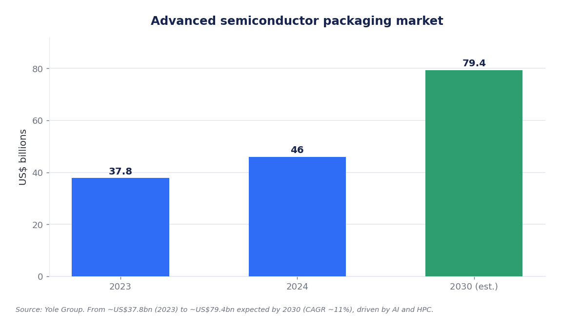
The most interesting detail is the internal recomposition. The largest segment remains mobile and consumer electronics, about 70% of 2024 revenues; but the one that is growing is telecommunications and infrastructure — essentially data centers — expected by Yole to grow at a compound annual rate of 14.9% between 2024 and 2030. Volume is still in smartphones; margin and growth are shifting to servers.
TSMC: packaging is no longer an ancillary service
TSMC's second quarter 2026 results, published on July 16, best illustrate the transformation.
| TSMC, second quarter 2026 | Value |
|---|---|
| Revenue | 40.20 billion dollars (+12% quarter-on-quarter) |
| Gross / operating margin | 67.7% / 60.3% |
| HPC platform | 66% of revenue (+20% quarter-on-quarter); smartphones at 22% |
| 2026 investments (guidance) | 60-64 billion dollars, raised from 52-56 |
| Capex for advanced packaging, test, and masks | 10-20% of total |
| Third quarter guidance | 44.6-45.8 billion, gross margin 65-67% |
The key figure is investments: at the high end, 20% of 64 billion means over twelve billion dollars in a year allocated to advanced packaging, testing, masks, and related items — the company does not disaggregate packaging alone — for an activity that, according to industry estimates collected by TrendForce, accounted for about 10% of the group's revenues in 2025. TrendForce also notes that the gross profitability of advanced packaging is still lower than the company average, but that prices are bringing it closer to that of logic processes: a historically low-value-added activity is becoming a second profit driver.
The queue shortens, but doesn't close
TrendForce's outlook for June 15, 2026, is this: TSMC's CoWoS capacity is expected to increase from approximately 75-80 thousand wafers per month at the beginning of 2026 to 120-140 thousand by the end of the year, with external partners — independent assemblers, or OSATs — adding another 50-60 thousand: an industry capacity close to 200 thousand wafers per month. The gap between supply and demand is thus expected to narrow from approximately 20% to about 10%: an improvement, not a solution, because by the end of 2026, one in ten requested chips will still be missing.
However, who gets that capacity also matters. According to industry reconstructions published by DigiTimes in December 2025, Nvidia would have booked over half of TSMC's CoWoS capacity for the 2026-2027 biennium, and major customers collectively over 85%: less than 15% would remain for the rest of the market. This detail explains why many announced AI chip projects never reach volume: the design is not missing, the assembly slot is.
Who profits downstream
The second quarter of 2026 brought record results for the two largest listed OSATs. Amkor Technology reported on July 27, 2026, revenues of 1.90 billion dollars, up 26% year-on-year, with a gross margin of 16.8%, net income of 174 million, and 0.70 dollars per diluted share. The relevant point: advanced packaging products accounted for 1.557 billion, i.e., 82% of revenues. 2026 investments are projected between 2.5 and 3.0 billion: for a company that bills 1.9 billion per quarter, this is a capex-to-revenue ratio like a foundry, not an assembler.
ASE Technology Holding, the world's leading OSAT, reported on July 9, 2026, second-quarter revenues of 191,064 million Taiwan dollars (6,050 million dollars), +26.7% year-on-year, with the assembly, test, and materials division at 126,148 million (+36.3%).
Not just TSMC: the game is open
Intel is moving decisively, not on silicon but on the package itself: according to TrendForce (March 18, 2026) the advanced packaging complex in Malaysia, internally known as Project Pelican, was 99% complete and expected to be operational by 2026, supporting both EMIB and Foveros. The most eloquent signal, however, came from the TSMC earnings call on July 16, 2026, where management said they welcomed alternative solutions like EMIB-T, because they alleviate CoWoS capacity constraints. When the market leader hopes competitors add capacity, the bottleneck is real.
In the background, a more radical change is being prepared: the transition from round 300-millimeter wafers to square panels. This is the essence of TSMC's CoPoS (chip on panel on substrate), with the first machinery deliveries in February 2026, qualification expected by June 2026, and ramp-up between 2028 and 2029. A panel wastes much less area than a disk when cutting large, rectangular packages; the obstacle is deformation: the wider the substrate, the more it tends to warp during thermal cycles.
Why it's also a geopolitical game
For years, Western industrial policy looked only at wafer fabs, ignoring that almost all advanced assembly was concentrated in East Asia. 2026 shows the course correction. Amkor has increased its investment in the Peoria, Arizona campus from 2 to 7 billion dollars — construction started in October 2025, CHIPS Act support up to 400 million in grants and 200 million in loans — and will assemble chips from the nearby TSMC factory on a turnkey basis, with Apple among the clients. In the same direction is TSMC's announcement of an additional 100 billion dollars in Arizona for 2-nanometer and beyond fabs and advanced packaging facilities.
What to watch in the coming quarters
The CoWoS supply-demand gap. The goal is to reduce it from approximately 20% to 10% by the end of 2026. If the gap closes faster, pricing power for packaging decreases; if it doesn't close, the scarcity shifts to the following year.
The gross margin of OSATs. This is the most honest thermometer of the supply chain: Amkor guided to 18.5-19.5% for the third quarter of 2026 from 16.8% in the second. If the climb continues, bargaining power shifts towards assemblers.
Demand concentration. If over half of the world's most advanced packaging capacity is booked by a single customer, the risk is not scarcity: it's that customer slowing down. On July 29, 2026, SK hynix published the best quarter in its history — operating profit of 60,542.6 billion won, margin of 76% — and the stock still lost 9.61% in Seoul: the result, though record-breaking, was below analysts' consensus (around 64,000 billion won according to LSEG SmartEstimate). The market did not punish the accounts; it repriced expectations for subsequent quarters.
The dates for CoPoS and EMIB-T. These are the two attempts to circumvent the bottleneck through different routes: a delay in both would extend scarcity beyond 2027.
The fundamental point remains: for fifty years, semiconductor progress has been measured by transistor size. A growing part of that progress, however, comes from package architecture, meaning how pieces are arranged, stacked, and connected. It is a technical change that has already shifted the profile of who profits in the supply chain.
Sources: Yole Group, «Advanced packaging market set to reach $79.4 billion by 2030» (02/09/2025); TSMC, Q2 2026 results and call (16/07/2026), via The Motley Fool transcript and slides from Investing.com; TrendForce on CoWoS wafer price (28/04/2026), on capacity and supply-demand gap (15/06/2026), on CoPoS (13/04/2026) and Intel plans (18/03/2026); Tom's Hardware on CoWoS roadmap; DigiTimes (10/12/2025) on capacity allocation; Amkor Technology (27/07/2026 and October 2025); ASE Technology Holding (09/07/2026); SK hynix, «2Q26 Financial Results», and CNBC (29/07/2026). Industry estimates are subject to revision. The Hub Finanza chart is for illustrative purposes.
Disclaimer: the information provided in this article is for informational purposes only and does not constitute personalized financial advice in any way. It is recommended to consult a qualified professional before making any investment decisions.